
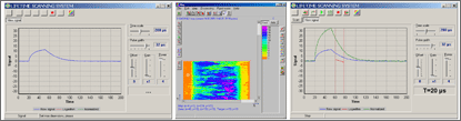
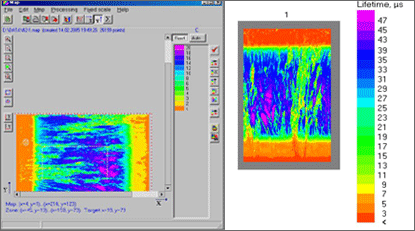
The device is designed for express non-destructive contactless local measurement of non-equilibrium charge carrier effective lifetime in silicon substrates, epi-wafers and solar cells at different stages of manufacturing cycle. It can be used for incoming and outcoming inspection of silicon ingots and wafers, tuning and periodic inspection of semiconductor and solar cell technology quality. Lifetime determination is based on measuring photoconductivity decay after pulselight photo-exciting with usage of reflected microwave as a probe.

■ No length restrictions for the silicon block
■ The system provides fast, non-contact measurements.
■ Automatic, Transmission system,continuous measurement
■ Simple, easy to cut head and tail
■ Cut position determination with given limit values
■ High cost-effective
■ Minority carrier lifetime test range:0.1μs-30ms
■ Scanning speed:2000mm/min
■ Size:215mm*215mm*500mm
■ Resistivity range:0.1-1000ohm.cm
■ Silicon block scanning pitch spacing:≥1mm
■ Accuracy:±3.5%,Signal Deviation≤2%